- The government notified the Rs 1,27,500-crore Semicon 2.0 scheme, which cuts capital subsidies for chip fabrication plants and adds fiscal support for makers of semiconductor equipment, chemicals, gases and raw materials for the first time.
- ISM 2.0 has an outlay of ₹1.27 lakh crore, with all pillars of categories being fungible insofar as the share of investments they may receive under the scheme.
- IT Minister Ashwini Vaishnaw stated that the reduction in central capital support for semiconductor fabrication projects from 50% under the first phase of the India Semiconductor Mission (ISM) to 40% under Semicon 2.0 will not make India less attractive to global investors.
- Vaishnaw highlighted the pace of execution under ISM 1.0, noting some projects moved from groundbreaking to commercial production within 13 months, and approvals in some cases were completed within 90 to 200 days.
- Semicon 1.0 provided 50% capital subsidy to semiconductor projects, but this has been reduced to 40% in phase 2, a change Mr. Vaishnaw said was due to increased enthusiasm among global players and additional support from State governments.
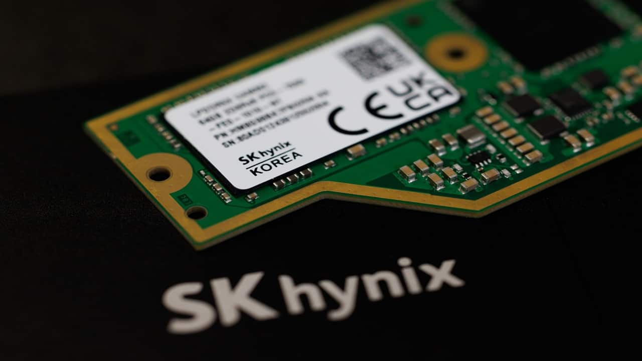
- Semicon 1.0 approved 12 projects across six states with investment commitments above ₹1.64 lakh crore. Three back-end units have started commercial production this year, including Micron's assembly-and-test plant, Kaynes Semicon and CG Semi's OSAT facility, all in Sanand, Gujarat.
- India's first fab, Tata Electronics' ₹91,000-crore plant at Dholera built with Taiwan's PSMC, is due to be commissioned in 2028.
India's IT Ministry has officially launched Semicon 2.0, a ₹1.27 lakh crore initiative aimed at bolstering the semiconductor ecosystem. The scheme reduces capital subsidies for chip fabrication from 50% to 40%, reflecting increased global confidence in India's chip manufacturing capabilities.23
The initiative encompasses six key pillars: design, machines and materials, fabs, packaging and testing, research and development, and talent development. Each pillar is designed to enhance various aspects of semiconductor production, with capital subsidies of up to 75% for research and development projects.

IT Minister Ashwini Vaishnaw emphasized the importance of making India a reliable player in the global semiconductor supply chain, stating, “People should feel dependent on India”. He noted that the reduction in subsidies would not deter global investors, as the overall incentive structure remains attractive.4
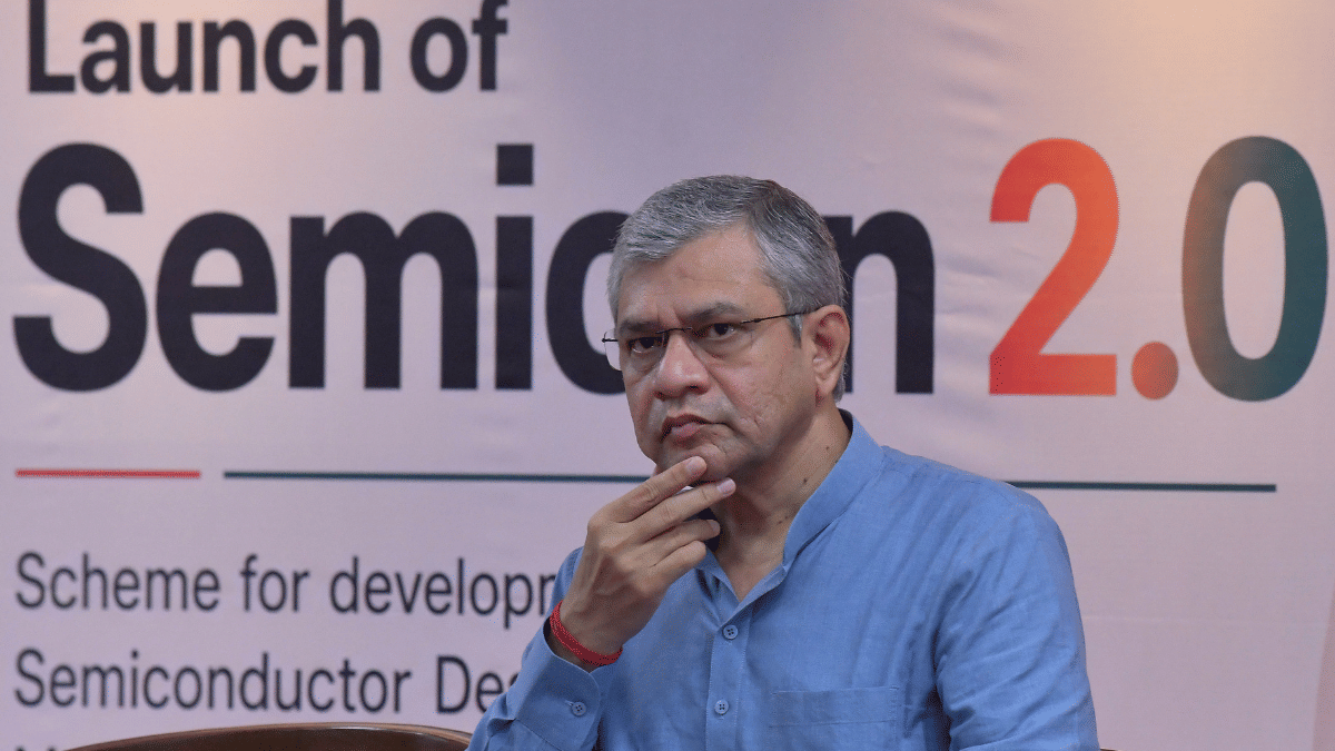
The scheme also mandates that strategically important chip designs be co-owned by a state agency, ensuring that critical intellectual property remains within India. “There is a significant level of confidence among the global semiconductor industry stakeholders that India is definitely the right place for making major investments in the coming decades,” Vaishnaw added.
With a focus on developing talent, the government aims to train one lakh design engineers over five years, up from the previous target of 85,000. This is part of a broader strategy to ensure India's strategic autonomy in electronics manufacturing, addressing both advanced and assembly sides of production.
“The scheme introduces six pillars including design, equipment, and talent development, with R&D subsidised up to 75% and talent projects up to 75%. Vaishnaw said global chipmakers moved from 'serious doubt' in 2022 to 'confidence' in India, citing execution pace like 13-month fab-to-production timelines.”